| |
All the technology you need for successful simulation
Key Benefits
• Acquire DDR simulation results and accurately predict simultaneous
switching noise
• Analyze compliance with DDR4, LPDDR4, and other memory interfaces
• Predict the BER
• Convert transitor-level SPICE models to power-aware IBIS models
The system engineer responsible for IO-SSO and the effects it has on the DDR
memory system will be happy to know that all the technology needed for successful
simulation is now available in a single suite of analysis tools, the Cadence® IO-SSO
Analysis Suite.
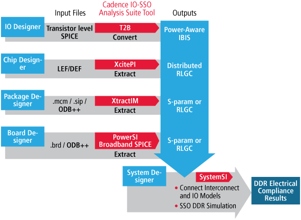
Figure 1. Cadence IO-SSO Analysis Flow
Design Flow
While the system designer is responsible for looking at the various topologies and
analyzing the effects of simultaneous switching outputs, there are a number of
interconnect models required to perform effective simulations. In addition, the
simulations will be much faster if performed with power-aware signal integrity (SI)
models over transistor-level SPICE models. The IO-SSO Analysis Suite allows the
designer to start with native design files for the I/O, chip, package, and PCB, and
either convert or extract those models into a format that can be dropped into the
Sigrity™ SystemSI™ topology editor.
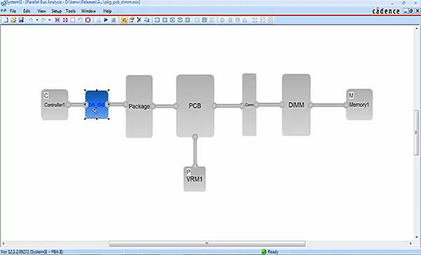
Figure 2. Die-to-die DDR4/LPDDR4 configuration in Sigrity SystemSI
Once the models are in the system topology editor, the system designer goes
through a process of connecting the models together. This process includes the
connections for signal, power, and ground. When the models are extracted using
the Sigrity XcitePI™, XtractIM™, and PowerSI® technologies, model connection
protocol (MCP) headers will appear in each model, making the connectivity much
more intuitive.
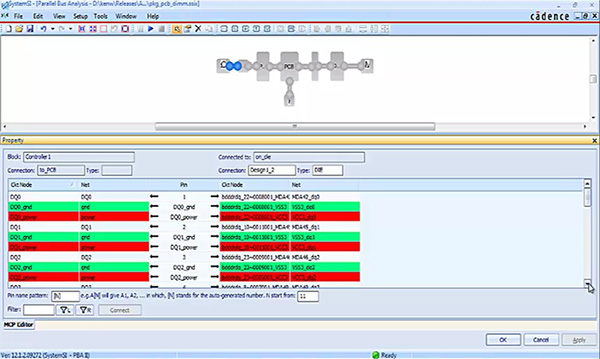
Figure 3. MCP file headers allow the MCP editor to quickly connect interconnect models
With the models connected in the topology editor, DDR simulation results can be
acquired. With power-aware IBIS models and interconnect models with coupled
signal, power, and ground, the simulation will include noise-causing ground bounce
and power droop. With simultaneous switching outputs, noisy power and ground
rails will actually change the waveforms of the signals. Only with this accurate
simulation of signal, power, and ground can accurate prediction of simultaneous
switching noise be accomplished.
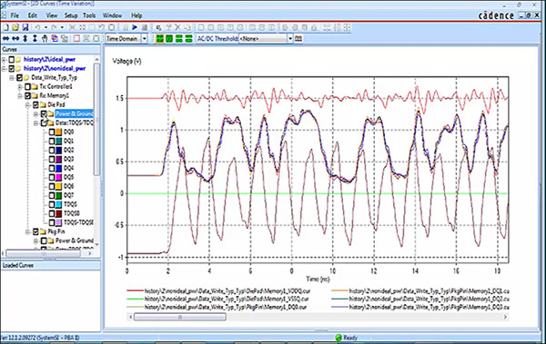
Figure 4. Power-aware time domain waveform results seen in Sigrity SystemSI
With accurate waveform capture, the SystemSI technology will carefully analyze the
data and report back the compliance with DDR4, LPDDR4, and other popular memory
interfaces. Captured in HTML format, the report data includes compliance criteria for
waveform quality, eye quality, timing, and delay.
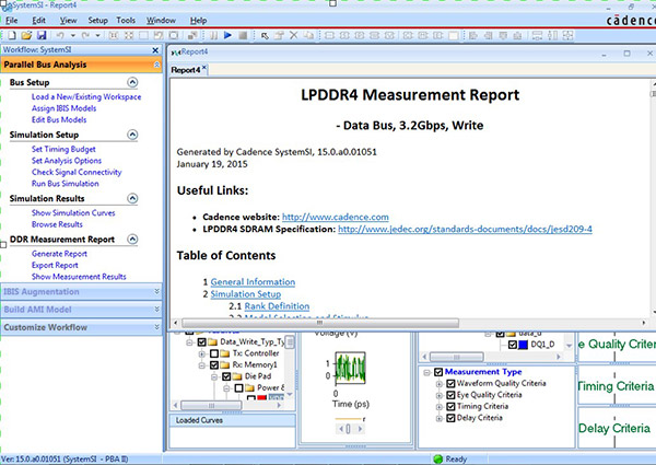
Figure 5. Detailed HTML reports provide pass/fail criteria based
on industry-standard compliance specifications
New to DDR and LPDDR compliance is the bit error rate (BER) test that is now part of
the DDR4 and LPDDR4 compliance requirements. Using techniques made popular in
Serial Link compliance testing, the SystemSI technology can run millions of data bits
on each signal and predict the bit error rate.
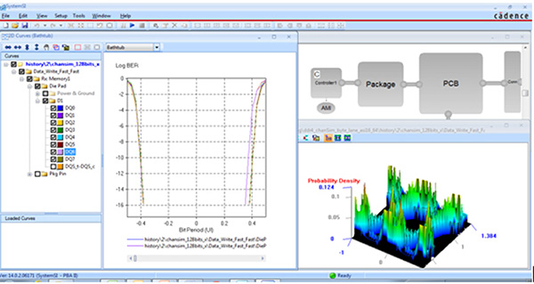
Figure 6. Bathtub curve used for BER calculations as seen in SystemSI
The IO-SSO Analysis Suite from Cadence provides an accurate and complete solution
from a single EDA vendor. Given the design data for the chip, package, and PCB, a
user of the IO-SSO Analysis Suite can extract all the fabrics into broadband
interconnect models where signal, power, and ground are all coupled. In addition,
transistor-level SPICE models can be converted to power-aware IBIS models. With
the I/O and interconnect models, DDR simulations can be run where the effects of
simultaneous switching outputs are considered in the compliance criteria. Analysis
data can be trusted as signoff quality as all the effects from non-ideal power and ground
have been considered.
|