| |
Quickly take designs from concept to production
Key Benefits
• Speeds designs from placement and routing through to manufacturing
• Includes powerful features such as design partitioning, RF design
capabilities, and interconnect design planning
• Production proven to increase productivity and help engineers quickly
ramp up to volume production
• TÜV SÜD “Fit for Purpose – TCL1” certified to meet ISO 26262 automotive
functional safety requirements
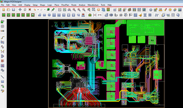
The Cadence® Allegro® PCB Designer
quickly takes simple and complex designs
from concept to production in a
constraint-driven design system to ensure
functionality and manufacturability.
Scalable technology allows designers to
cost-effectively match all current and future
technological and methodological needs for
teams, organizations, and projects of all sizes
and complexities.
The industry's latest bleeding-edge high-speed
design, RF antenna, flex-circuitry, and design
for manufacturing (DFM) technology in the
Allegro PCB Designer gives you what you need
to deliver the innovative products your customers
demand. And the advanced design reuse and
productivity features give you the advantage you
need to beat your competitors to market. |
Speed designs from placement and routing
through to manufacturing with powerful
features such as design partitioning, RF
design capabilities, and interconnect
design planning. |
Automotive TCL1 Certified for ISO 26262
The industry’s first PCB design and verification flow to achieve “Fit for Purpose -
Tool Confidence Level 1 (TCL1)” certification enables you to meet stringent ISO
26262 automotive safety requirements. The flow includes everything from design
authoring to simulation to physical realization and verification using the PSpice®,
Allegro, and OrCAD® product suites. The high-performance design entry,
simulation, and layout editing tools provide an integrated environment for design
engineers to validate the safety specifications against individual circuit specifications
for design confidence. For information on the safety manuals, Tool Confidence
Analysis (TCA) documents, and compliance reports from TÜV SÜD, download the
Functional Safety Documentation Kits through Cadence Online Support.
Features
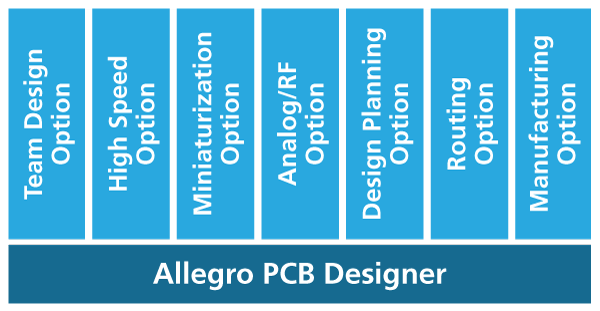
• Provides a scalable, full-featured PCB design solution
• Enables a constraint-driven design flow to reduce design iterations
• Integrated DesignTrue DFM technology providing real-time DFM checks
• Provides a single, consistent, front-to-back constraint management environment
• Minimizes design iterations and lowers overall cost for flex and rigid-flex designs
with advanced rigid-flex design capabilities
• Enables dynamic concurrent team design capability to shorten design cycle by
dramatically reducing time spent on routing, tuning, and optimization of signals
• Delivers an integrated RF/analog design and mixed-signal design environment
• Provides interactive floorplanning and component placement
• Provides design partitioning for large, dispersed development teams
• Enables real-time, interactive push/shove etch editing
• Allows real-time plowing/healing with dynamic shape technology
• Manages net scheduling, timing, crosstalk, layer set routing, and geometric
constraints
• Provides proven PCB router technology for auto-routing of random signals
• Enables hierarchical route planning to accelerate design completion
• Shortens interconnect planning and routing time for dense designs with
high-speed interfaces
• Provides a comprehensive, powerful, easy-to-use suite of tools to assist
designers with an efficient and successful handoff to manufacturing:
• DFM Checker for signoff against company/manufacturing-partner-specific
rules
• Documentation Editor for reducing fabrication and assembly documentation
time up to 70%
• Panel Editor for communicating assembly panel design intent to manufacturing
partners
• Outputs design data in a variety of manufacturing formats
|