| |
Advanced system-in-package implementation including die/BGA
interface optimization
Key Benefits
• Supports complex 3D SiP package design
• Advanced support for wirebond, flip-chip, and wafer-level chip-scale packaging
• Supports efficient and chip IP secure distributed co-design for chip/package
optimization
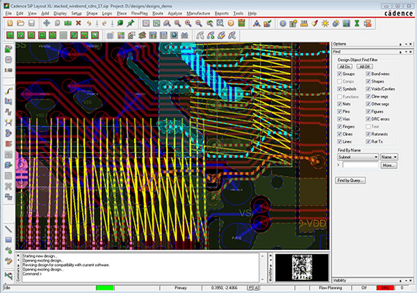
Cadence® SiP Layout provides a complete constraint- and rules-driven substrate
layout environment, including full 3D design visualization, verification, and editing
capabilities. Direct integration with Cadence OrbitIO™ Interconnect Designer provides
the rapid implementation of proven interconnect pathways and die/BGA assignments.
Cadence SiP Layout Solution
Cadence SiP Layout is a complete physical design and manufacturing verification solution
for complex 3D SiP package design, including die bump array/BGA integration refinement
using die abstracts. Supporting all popular package interconnect and assembly methodologies,
SiP Layout provides comprehensive constraint-driven layout of the package substrate. Since
it must operate in a 3D world, SiP Layout allows stack assembly optimization with 3D layout
and editing. It also contains a powerful set of auto-interactive routing features that speed timing
closure of critical interconnects such as DDR3, etc. Intelligent automated flip-chip die breakout
reduces time-consuming and tedious manual breakout. Comprehensive DFM and DFA checking
and modification improves substrate yield and prevents manufacturing assembly issues. Design
review documentation and debug, followed by direct manufacturing tapeout, completes the
package.
Features
• Provides 3D die stack creation and editing for rapid stack assembly and optimization
• Supports PiP-, PoP-, and interposer-based assembly architectures
• Enables connectivity assignment to minimize layer usage based on SI analysis
• Includes solid model 3D design viewer with snapshots for design review
• Performs 3D wirebond verification and DRC with Kulicke- and Soffa-verified wire profiles
• Supports bi-directional ECO and LVS flow for full co-design environment profiles
• Includes a comprehensive suite of DFM/DFA preparation rules
• Direct integration with OrbitIO Interconnect Designer for detailed package interconnect
pathway implementation
• Supports distributed die/BGA interconnect refinement using XML-based die abstracts
compatible with Cadence Innovus™ and Virtuoso® solutions
|