| |
Create an optimum correct-by-construction pin assignment for
FPGA-PCB co-design
Key Benefits
• Complete, scalable technology for FPGA/PCB co-design for ideal
correct-by-construction pin assignment
• Scalable FPGA/PCB co-design solution from OrCAD Capture to Allegro GXL
• Shorter time for optimum initial pin assignment accelerates PCB design
schedules
• TÜV SÜD “Fit for Purpose – TCL1” certified to meet ISO 26262 automotive
functional safety requirements
The Cadence® Allegro® FPGA System Planner offers a complete, scalable technology
for FPGA/PCB co-design that allows users to create an ideal correct-by-construction
pin assignment. FPGA pin assignment is synthesized automatically based on
user-specified, interface-based connectivity, FPGA device pin assignment rules, and
placement of FPGAs on the PCB. With automatic pin-assignment synthesis, users avoid
manual error-prone processes while shortening the time to create initial pin
assignment that accounts for FPGA placement on the PCB. This unique
placement-aware pin assignment approach eliminates unnecessary physical design
iterations that are inherent in manual approaches while shortening the design cycle
time.
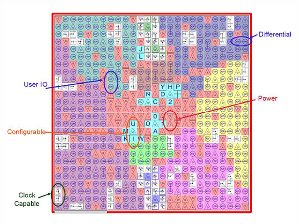
Color-coded map of the I/Os of a multi-bank FPGA with different types
of configurable pins
By enabling placement-aware pin-assignment synthesis—which is FPGA device rules
accurate—the Allegro FPGA System Planner offers a unique set of capabilities for
FPGA/PCB co-design. It provides a floorplan view to place components in the FPGA
system and allows users to specify connectivity between components within the FPGA
subsystem at a higher level through interface definitions. With its placement-aware
pin-assignment synthesis, the Allegro FPGA System Planner enables users to explore
their FPGA-based architecture and to create an optimum correct-by-construction pin
assignment for either production or prototype designs that use FPGAs.
Automotive TCL1 Certified for ISO 26262
The industry’s first PCB design and verification flow to achieve “Fit for Purpose - Tool
Confidence Level 1 (TCL1)” certification enables you to meet stringent ISO 26262
automotive safety requirements. The flow includes everything from design authoring
to simulation to physical realization and verification using the PSpice®, Allegro, and
OrCAD® product suites. The high-performance design entry, simulation, and layout
editing tools provide an integrated environment for design engineers to validate the
safety specifications against individual circuit specifications for design confidence.
For information on the safety manuals, Tool Confidence Analysis (TCA) documents,
and compliance reports from TÜV SÜD, download the Functional Safety
Documentation Kits through Cadence Online Support.
Features
• Accelerates integration of FPGAs with Cadence PCB design creation environments
• Eliminates unnecessary, frustrating design iterations during the PCB layout process
• Eliminates unnecessary physical prototype iterations due to FPGA pin assignment errors
• Reduces PCB layer count through placement-aware pin assignment and optimization
• Enables interface-based connectivity definition for the FPGA system
• Enables placement-aware pin assignment synthesis that is FPGA-DRC accurate
• Allows architectural exploration for FPGA system
• Speeds ASIC prototyping using FPGAs
|